Papanikolas Group
Ultrafast Spectroscopy and Ultrafast Microscopy
Papanikolas Group
Ultrafast Spectroscopy and Ultrafast Microscopy


Ultrafast Microscopy:
Visualization of Charge Carrier Dynamics in Nanostructures

Group Members
Overview


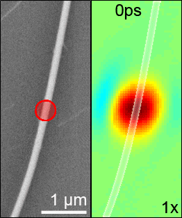
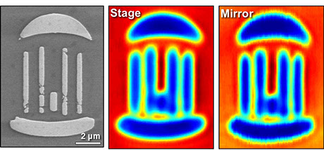
We are developing ultrafast microscopy techniques for studying the electronic dynamics of individual nanoscale objects with combined spatial and temporal resolution, enabling charge carrier behavior to be correlated with specific structural features. By exciting a structure in one location and probing it in another, we can directly observe the motion of charge carriers as they move through nanowires and other structures. Our focus is on nanomaterials targeted for use in a variety of nanotechnologies, including nanowire photovoltaics relevant to solar energy conversion, nanoelectronics and photonics. Ultrafast imaging methods are combined with scanning electron microscopies that reveal structural details. Finite element simulations (FDTD and FDFD) provide insight into the physical factors that govern carrier behavior.
Research Directions
Explore Our Publications
Collection of papers on selected topics. PDF files are book-marked for easy navigation
Visualization of Carrier Dynamcis in Silicon Nanowires
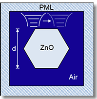
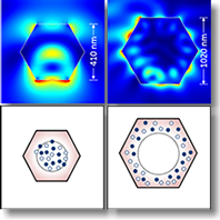
ZnO - Carrier Dynamics and Optical Resonator Modes
Finite-Element Simulations
Computer modeling of the physical phenomena are integral part of our studies. We are developing finite element models (FDTD and FDFD) to to gain insight into the relationship between structural features and dynamical behavior. These models guide our intuition and provide direct input into the analysis of the experimental data. We have modeled the optical resonator modes in tapered ZnO nanorods, and have simulated charge carrier dynamics (e.g. charge separation recombination, diffusion and drift) in p-i-n nanowire junctions.
 Effect of Strain on Nanowire Carrier Dynamics
Straining nanowires through mechanical deformation (e.g. pulling or bending) can alter band energies and symmetries, thus providing a novel route to new device applications. We are examining the spatial variation in carrier dynamics in strained nanowire structures.
 Carrier Motion in Complex Nanowire Structures
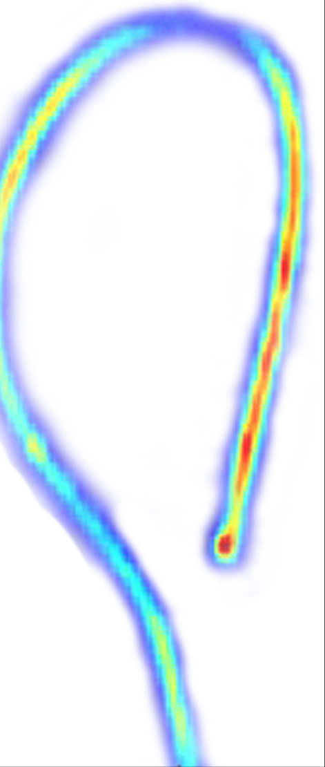
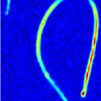
We are using ultrafast microscopy to visualize charge carriers as they move through the complex geometrical shapes (e.g. such as kinks and constrictions) in individual structures.
 Spatially Resolved Dynamics at Low Temperature
Experiments at low temperature reveal detail that is normally masked at higher temperatures. We are conducting experiments at temperatures as low 8 K to learn about the spatial variation in the energy landscape and its affect on the carrier dynamics.

Experimental and Theoretical Methods
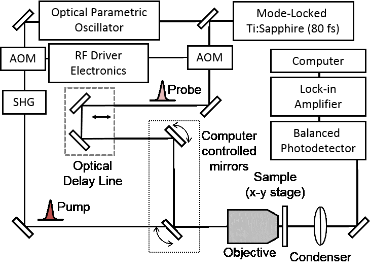
Microscopy Development
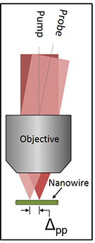
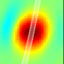
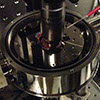
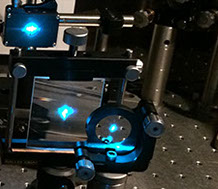
A major effort in our lab is directed at the development of the ultrafast microscopy technique. A schematic of our home-built pump-probe microscope is shown at the left. A model-locked Ti:Sapphire laser and optical parametric oscillator are used to generate the pump and probe beams. The probe is passed through an optical delay stage and recombined with the pump. The two pulses are then directed into the back aperture of a microscope objective, which focuses them to diffraction limited spots. The probe beam is collected after the sample and pump-induced changes in its intensity are detected using a lock-in amplifier. The technique is remarkably sensitive and signals from Silicon nanowires as small as 15 nm in diameter are routinely detected. A pair of mirrors control the angle of the probe beam at the back aperture of the microscope objective, enabling the pump and probe beams to be positioned at different points in the sample.
Papanikolas Group
Department of Chemistry
University of North Carolina at Chapel Hill