Papanikolas Group
Ultrafast Spectroscopy and Ultrafast Microscopy
Papanikolas Group
Ultrafast Spectroscopy and Ultrafast Microscopy


Ultrafast Microscopy:
Visualization of Charge Carrier Dynamics in Nanostructures
Group Members
Carrier Dynamics in Si Nanowires


We are applying the ultrafast microscopy methods developed in our laboratory to the characterize the carrier dynamics (e.g. electron-hole recombination, charge separation, diffusion and drift) in Si NWs. There is intense interest in nanowires, particularly Si NWs, for use in a wide variety of nanotechnologies. Ultrafast microscopy provides a unique view of the nanowire behavior that is difficult (or impossible) to obtain using conventional experimental methods. These projects are being pursued in partnership with Cahoon group, who are experts in the growth, characterization and manipulation of nanowire materials.
Research Highlights

James Cahoon


Comparison of Microscopy and Transient Absorption
Two back-to-back papers that appeared in J. Phys. Chem. C showed that transient absorption methods tend to overestimate the electron-hole recombination rate due to averaging over bent structures in the sample. The observation motivated our investigation of strain effects in nanowire dynamics.
Watching Electrons Move in Nanowires
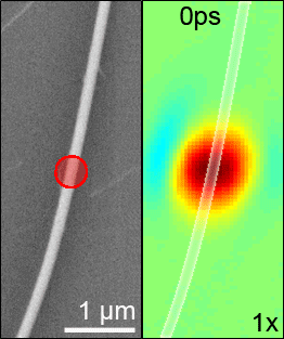
The movement of electrons through objects is central to the function of all electronic devices. Using a microscope that is capable of exciting a single object in one place, and probing it in another, we have imaged carrier motion (animation, right). Electrons and holes are created at the location of the red circle by photoexcitation with a femtosecond laser pulse that has been focused to a diffraction limited spot by a microscope objective. As time increases, the carriers recombine and the intensity of the spot decreases (note the scaling factor in lower right corner). As this happens, the spot also elongates along the nanowire reflecting the motion of the charge cloud. By analyzing the rate of growth of the charge cloud we can determine the carrier diffusion constant at a specific point in a single nanostructure. The blue spot at longer times is the result of local heating by the pump pulse. <Read>
Spatially Resolved Charge Carrier Recombination in Nanowires Strained by Bending Deformation
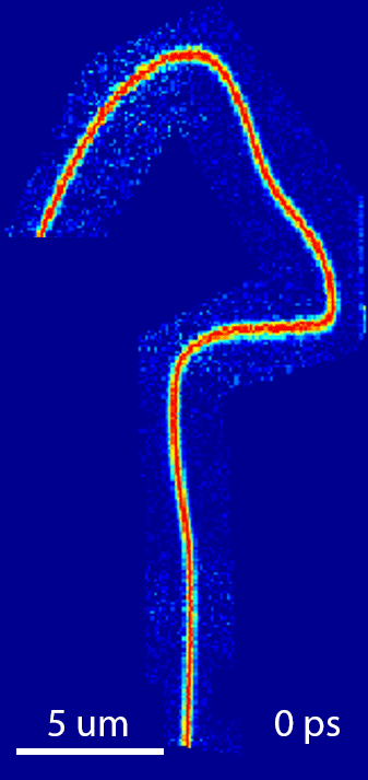
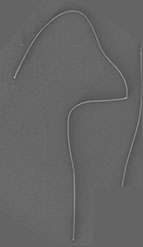

The combined spatial and temporal resolution of pump-probe microscopy offers a unique opportunity to study nanostructures that are strained through mechanical deformation. We have recently investigated the effect of inhomogeneous strain on the electron-hole recombination dynamics in bent Silicon nanowires. The movie at the left shows the free carrier population in a nanowire that was bent upon transfer to the substrate. The carrier population decays more rapidly in the bent regions of the structure. Experiments performed on flexible substrates (i.e. PDMS) reveal that the recombination rate returns to values commensurate with the straight regions when the NW is straightened. This reversible behavior indicates that the faster recombination is not simply due to the introduction of defects into the lattice, but rather the result of intrinsic changes to the nanowire band structure in the vicinity of the bend. <Read>
Imaging Charge Separation in a
Nanowire p-n Junction
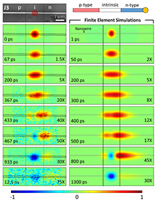
The electric field created at the junction between p-type and n-type Silicon is central to the separation of electrons and holes in photovoltaic devices. We have used spatially-separated pump-probe microscopy to image charge separation in a Si nanowire encoded with an axial p-type/intrinsic/n-type (p-i-n) junction. Finite element simulations provide a detailed understanding of the carrier drift/diffusion and recombination in the junction, revealing that the evolution of the charge distribution at early times is dominated by carrier-carrier interactions. <Read>
Papanikolas Group
Department of Chemistry
University of North Carolina at Chapel Hill